(China (Mainland))

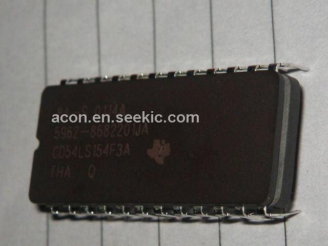
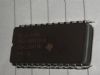
Product Summary
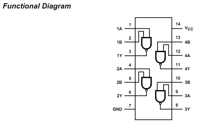
The CD54LS154F3A is a logic gate utilizing silicon gate CMOS technology to achieve operating speeds similar to LSTTL gates with the low power consumption of standard CMOS integrated circuits. The CD54LS154F3A has the ability to drive 10 LSTTL loads. The CD54LS154F3A logic family is functionally pin compatible with the standard 74LS logic family.
Parametrics
CD54LS154F3A absolute maximum ratings: (1)DC Supply Voltage, VCC: -0.5V to 7V; (2)DC Input Diode Current, IIK For VI < -0.5V or VI > VCC + 0.5V:±20mA; (3)DC Output Diode Current, IOK For VO < -0.5V or VO > VCC + 0.5V: ±20mA; (4)DC Output Source or Sink Current per Output Pin, IO For VO > -0.5V or VO < VCC + 0.5V: ±25mA; (5)DC VCC or Ground Current, ICC or IGND:±50mA.
Features
CD54LS154F3A features: (1)Buffered Inputs; (2)Typical Propagation Delay: 7ns at VCC = 5V, CL = 15pF, TA = 25℃; (3)Fanout (Over Temperature Range): Standard Outputs: 10 LSTTL Loads; Bus Driver Outputs: 15 LSTTL Loads; (4)Wide Operating Temperature Range: -55℃ to 125℃; (5)Balanced Propagation Delay and Transition Times; (6)Significant Power Reduction Compared to LSTTL Logic ICs; (7)Alternate Source is Philips/Signetics; (8)HC Types: 2V to 6V Operation; High Noise Immunity: NIL = 30%, NIH = 30% of VCC at VCC = 5V; (9)HCT Types: 4.5V to 5.5V Operation; Direct LSTTL Input Logic Compatibility, VIL= 0.8V (Max), VIH = 2V (Min); (10)CMOS Input Compatibility, Il ≤ 1μA at VOL, VOH.
Diagrams